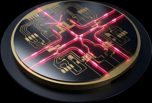
Next Gen CMOS Photonics

A silicon-compatible photonics platform that brings high-speed, low-energy electro-optic performance into standard silicon manufacturing — without specialized fabs, bonding steps, or yield penalties.

01 The Problem

The next generation of photonics needs both better manufacturability and physics

AI data centers, cloud infrastructure, and telecom networks are pushing photonic circuits beyond the practical limits of conventional silicon photonics. Silicon is manufacturable at scale, but carrier-based modulation creates limited bandwidth, optical loss, non-linearity, and power penalties at next-generation data rates.

Existing high performance alternatives can improve modulation physics, but often require nonstandard processes, bonding steps, or specialized photonic fabs. The industry needs both silicon-scale manufacturing and electro-optic performance.


02 Our Solution

The MoRF CHIP — a CMOS compatible photonic platform

MoRF's proprietary material stack enables a direct, field driven modulation that is fast, linear, and has low-loss. The platform supports a path to bandwidths above 100 GHz, energy consumption of 1/10th, higher-order modulation formats, and reduced DSP burden compared with conventional silicon modulation.

MoRF's process is designed for CMOS-compatible integration as an active photonics layer, with a roadmap toward foundry PDK adoption and high-yield manufacturing through standard silicon infrastructure.


03 The Technology
MoRF photonic chip — circular wafer with red laser circuitry

Photonic Components

  • Waveguide
  • Pockels Modulator
  • 2nd Harmonic Generation
  • Telecom, Compute, and Quantum

Platform is made out of MoRF III-V material and any Substrate (Si \ Glass \ Metal)

Advantages

  • 4x Modulation Speed
  • 10x Energy Cost Reduction
  • 10x BOM Price Reduction
  • Form Factor Reduction
  • Silicon Fabrication Yield